TSMC Slightly Reduces the Price Increase for Its 2 nm Wafers
In August, a report indicated that TSMC planned to increase the price of its 2 nm (N2) silicon wafers by 50%, bringing the cost to $30,000 per unit—up from around $20,000 for the 3 nm (N3P) wafers.
However, according to new information from Taiwan, the increase will be much less than initially expected.
TSMC: A Moderated Increase Between 10% and 20%
According to the latest report, TSMC will indeed raise its prices, but by only 10% to 20%. Thus, the price of 2 nm wafers will range between $22,000 and $24,000, significantly lower than the previously mentioned $30,000.
This moderation could help mitigate the price increases anticipated for high-end smartphones launching in 2026, which will utilize this new manufacturing process.
Other advanced nodes—3 nm, 4 nm, 5 nm, 6 nm, and 7 nm—are also expected to see slight increases, averaging a few percent depending on the client.
The initial information came from EE Times, which reported a record price hike unprecedented during a generational transition. Had this been true, it would have marked the first time a technological leap resulted in an increase in cost per transistor, indicating a slowdown in miniaturization.
The correction of these estimates implies that the cost per transistor will remain stable, preserving the competitiveness of the new node.
US-Made Chips Will Be More Expensive
According to Investors.com, 3 nm wafers are currently selling for between $25,000 and $27,000, which aligns with the expected 10% to 20% increase to reach $30,000.
The report also notes that advanced production lines (3 nm to 7 nm) are operating at full capacity, while older nodes (28 nm, 40 nm, 65 nm, 90 nm) are underutilized.
TSMC’s US factories will apply a price increase of 5% to 20%, as confirmed by AMD CEO Lisa Su. Some sources even indicate that 4 nm chips produced in Arizona currently face a 30% markup.
This difference is attributed to higher production costs in the US, which reduce the foundry’s gross margins by 2% to 3%. TSMC aims to maintain a margin rate of 53%, deemed necessary to finance its massive investments in research and capacity expansion.
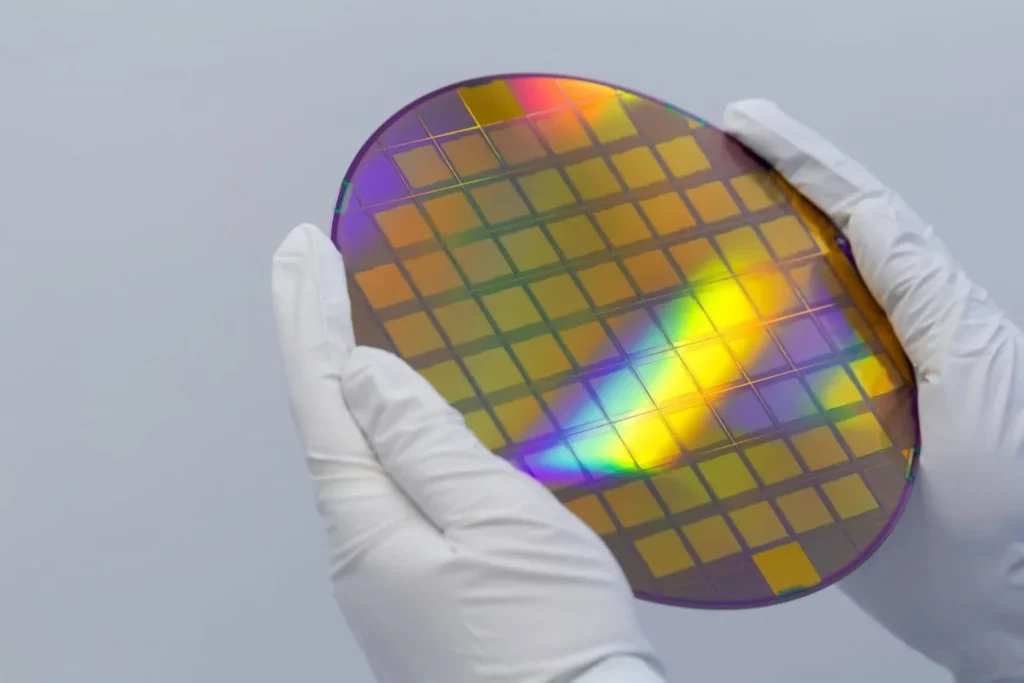
2 nm Process: A New Generation of Transistors
The 2 nm node introduces a new transistor architecture: Gate-All-Around (GAA). This technology employs horizontally stacked nanosheets, allowing the control gate to completely envelop the channel.
The results include:
- Reduced current leakage,
- Improved energy efficiency,
- And enhanced performance at the same voltage.
These advancements will enable future 2 nm processors—from Apple, Qualcomm, MediaTek, AMD, or Nvidia—to be faster and more energy-efficient.
Nvidia Supports TSMC’s Price Increase
Nvidia CEO Jensen Huang publicly endorsed TSMC’s decision to adjust its prices: “The value of what TSMC produces is immense… A price increase is natural and consistent with the value they provide.” This endorsement weighs heavily, coming from a prominent client in the new age of artificial intelligence.
In Q2 2025, TSMC achieved a record market share of 70.3% in the foundry sector, far ahead of Samsung Foundry, which holds only 7.3%. This lead is attributed to the reliability of the 3 nm process and the trust of major chip designers from Apple to AMD.
What Comes After 2 nm: Introducing A16 (1.6 nm)
TSMC plans to commence mass production of the A16 node in 2026. The “A” stands for angstroms—1 nanometer equals 10 angstroms—indicating that 16 angstroms equals 1.6 nm. This future node will unveil a significant innovation: the Super Power Rail, TSMC’s version of Backside Power Delivery.
Power delivery lines will be located at the back of the wafer, freeing up surface space for transistors. Expected gains include +8% to +10% in performance and −15% to −20% in energy consumption at equal power.
The A14 (1.4 nm) process is already slated for 2028, marking the next step in miniaturization.