TSMC: 2 nm chips at $30,000 each, the era of GAA transistors begins
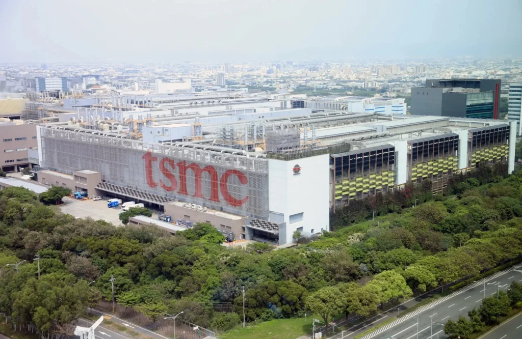
The Taiwanese foundry giant, TSMC, is on the verge of a historic milestone in the semiconductor industry. Starting in 2026, TSMC plans to produce 60,000 2 nm wafers per month, spread across four fully operational manufacturing sites.
This generation represents a significant technological shift, particularly through the adoption of Gate-All-Around (GAA) transistors and an unprecedented transistor density.
A Dramatic Increase in Wafer Prices
As performance advances, so do prices: each 2 nm wafer will cost $30,000, marking a 50% increase compared to the $20,000 cost of 3 nm wafers. This spike in costs reflects both the technical complexity of the 2 nm process and the heightened demand from AI and mobility giants.
According to internal reports, production requests (or tapeouts) for 2 nm are already exceeding those observed in the early years for the 5 nm and 3 nm nodes.
This indicates a rapid and extensive adoption of this technology by market leaders.
Tapeout: When Production Really Begins
For context, a tapeout refers to the moment when a company, such as Apple, Nvidia, or Qualcomm, sends the final design of its chip to the foundry to commence manufacturing. These TSMC clients, already deeply invested in the development of 2 nm nodes, are ready to move their next-generation chips into the industrial phase.
Why is 2 nm a Revolution?
The engraving node size (in nm) directly dictates the size of the transistors integrated into a chip. The smaller this size, the more transistors can be placed in a given area. The result: more power and less energy consumption.
Here’s a comparison of transistor density (MTr/mm²):
- TSMC 5 nm: approximately 130 to 170 million transistors per mm²
- TSMC 3 nm: approximately 190 to 220 million per mm²
This means a 3 nm chip can hold up to 46% more transistors than a 5 nm chip, translating into better energy efficiency and improved performance.
GAA: The New Transistor Architecture
With 2 nm engraving, TSMC introduces GAA (Gate-All-Around) transistors for the first time. Unlike current FinFET transistors, the channel is fully surrounded by the gate, reducing current leakage and enhancing switching power.
This marks a major shift in semiconductor design, as it increases electrical control over current in transistors, a crucial breakthrough for achieving a new level of miniaturization without sacrificing stability or power consumption.
What Lies Beyond 2 nm? Moving Towards A14…

TSMC has already outlined the next step in its roadmap: 1.4 nm engraving expected in 2028. However, the manufacturer will abandon the nanometer notation in favor of a new unit: the ångström (Å).
1 nanometer equals 10 Å. Thus, the 1.4 nm engraving node will be renamed A14 (14 ångströms). This change in terminology aims to better reflect the atomic advancements in the manufacturing process, now at a nearly molecular scale.
What Does This Revolution Mean for Smartphones?
With 2 nm chips expected in high-end smartphones as early as 2026, the promise is enticing: increased battery life, enhanced AI capabilities, reduced heat output, and greater miniaturization of components.
However, at $30,000 per wafer, the final production costs will inevitably impact device prices, which could amplify the differentiation between ultra-premium “Pro” models and more accessible variants, particularly within the Apple or Samsung ranges.